
Home
Page
STM32 Page
INDEX
INTRODUCTION
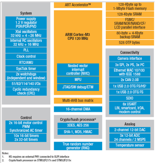
The ARM® Cortex-M3-based STM32 F2 series uses ST’s advanced 90 nm NVM process technology with the innovative adaptive real-time memory accelerator (ART Accelerator™) and multi-layer bus matrix. This offers an unprecedented trade-off in price and performance.
New STM32 F2 series offers 30 new devices; delivers 150DMIPS for high-performance power-sensitive applications.

New STM32 F-2 Series
Target Applications
PinOut compatibility from STM32F2xx to STM3F1xx
Evaluation Board
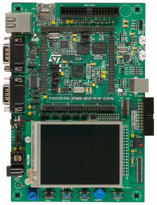
ST provides an evaluation board allowing full access to the STM32 F-2 series features such as external memories, Ethernet, the two USB OTG connectors, touchscreen TFT display, CMOS camera and audio output.
STM32 Page
INDEX
STM32 official page: http://www.st.com/internet/mcu/subclass/1520.jsp
Introduction
Price and Availability
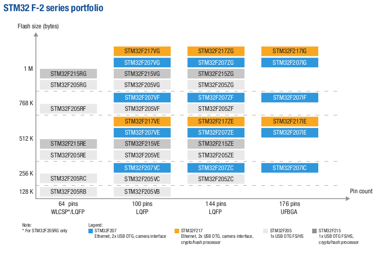
Portfolio
PinOut compatibility from STM32F2xx to STM32F1xx
Evaluation Board
Software, Application Notes, Manuals, etc
Brochures
Getting started with STM32F20xxx/21xxx MCUhardware development
Introduction
Price and Availability
Portfolio
PinOut compatibility from STM32F2xx to STM32F1xx
Evaluation Board
Software, Application Notes, Manuals, etc
Brochures
Getting started with STM32F20xxx/21xxx MCUhardware development
INTRODUCTION
The ARM® Cortex-M3-based STM32 F2 series uses ST’s advanced 90 nm NVM process technology with the innovative adaptive real-time memory accelerator (ART Accelerator™) and multi-layer bus matrix. This offers an unprecedented trade-off in price and performance.
New STM32 F2 series offers 30 new devices; delivers 150DMIPS for high-performance power-sensitive applications.
New STM32 F-2 Series
ST’s new leading-edge
STM32 F-2 microcontroller series combines ST’s advanced 90nm process
technology with the Company’s innovative Adaptive Real-Time memory
accelerator (ART Accelerator™) to unleash the Cortex-M3 core’s maximum
processing performance.
The STM32 F-2 MCUs achieve leading-edge performance of 150 Dhrystone MIPS when executing code from Flash at 120MHz, which is the maximum performance possible from the Cortex-M3 processor at this frequency.
The series also offers CoreMark-confirmed 200uA/MHz dynamic power consumption.
In addition to offering on-chip memory densities that are among the highest of any Cortex-M3 based MCUs available, the new series provides enhanced support for imaging, connectivity, security, audio and control applications.
For many applications, the STM32 F-2 MCUs offer the perfect balance
between performance, dynamic power consumption and cost, which has been
confirmed with the news that more than 20 of ST’s customers are
currently ramping up manufacturing of new products enabled by this new
STM32 family.
“This series is a major addition to the STM32 platform and reinforces ST’s leadership in the market for Cortex-M3 MCUs,” added Buffa. “ST’s proprietary 90nm process and the development of the ART Accelerator enable perfectly optimized processor-memory interactions with a performance equivalent to zero wait states, taking the performance of the Cortex-M3 core to its natural limits.”
The addition of more than 30 new devices in the F-2 series brings the total number of STM32 microcontrollers to 180 pin- and software-compatible devices sharing a common pool of peripherals, and delivering the advanced performance, high efficiency and convenience of the industry-standard Cortex-M3 processor.
Production samples of the STM32 F-2 series are available now to OEM customers with widely availability in Q1 2011.
Prices for the STM32-F2 series begin from $3.18 for the STM32F205RBT6 with 128 Kbytes of Flash and 64 Kbytes RAM in the LQFP64 package, for orders of more than 10,000 units.
Target Applications
- Consumer and Mobile applications, due to its performance, 1.65V support, audio-class architecture, and small WLCSP64 package;
- Industrial and Medical applications, due to rich connectivity peripheral sets, encryption, processing power, advanced timers and large Flash and SRAM memory.
Industry-Leading Performance
- 150 DMIPS (Dhrystone MIPS) at 120MHz;
- CoreMark™-confirmed fastest Cortex-M3 microcontroller, at 120MHz, delivering 1.905 CoreMark/MHz (228.60 CoreMark at 120MHz) performance, executing from embedded Flash memory;
- Seven-layer multi AHB bus matrix for seamless and efficient operation, even when several high-speed peripherals are operating simultaneously;
- Two separate blocks of SRAM located on the bus matrix allow simultaneous memory access from different bus masters
- 16 DMA channels.
Power Efficiency
- CoreMark-confirmed 200uA/MHz dynamic power consumption.
- Voltage range to further reduce power consumption – 1.65V to 3.6V for the WLCSP64 package, 1.8V to 3.6V for the other four packages
- Advanced low-power modes and features allowing VBAT mode, allowing consumption of less than 9uA with RTC (Real-Time Clock) turned on, and less than 15uA with memory preservation of 4 Kbytes of battery-backed SRAM.
- 1% internal RC oscillators
Advanced Peripherals
- 528 bytes of OTP (One-Time-Programmable) memory, allowing storage of critical data, such as Ethernet MAC addresses or encryption keys
- Parallel CMOS-camera sensor interface (8 to 14 bit parallel, up to 48 Mbyte/s at 48 MHz)
- Connectivity
2 x USB Full-Speed OTG interfaces, one supporting USB High Speed (480 Mbit/s) with dedicated DMA
1 x Ethernet MAC 10/100 with IEEE1588 PTP hardware support
2 x CAN 2.0B active
3 x SPI running at up to 30 Mbit/s
6 x USART running at up to 7.5 Mbit/s
3 x I2C
2 x I2S (Audio-class architecture)
External Memory Interface running up to 60MHz and supporting Compact Flash, SRAM, PSRAM, NOR, NAND memories and LCD - Control
2 x motor-control timers
12 x general-purpose timers
2 x 32-bit timers
2 x WDG timers
3 x 12-bit ADC (24 ch), 2 MSPS and up to 6 MSPS in interleaved mode
2 x 12-bit DAC
POR/PDR/PVD
- Fast GPIO (60 MHz toggling speed)
- RTC with hardware calendar support
- True random number generator
- Encryption
Crypto/Hash processor and Analog True Random Number Generator
Encryption block includes hardware acceleration for AES 128, 192, 256, Triple DES, HASH (MD5, SHA-1)
Packages
- LQFP64, LQFP100, LQFP144, UFBGA176, plus the WLCSP64 (less than 4 x 4mm) for applications where board space is limited
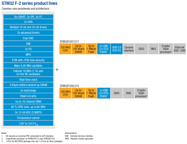
F-2 Series Variants
- STM32F205 devices provide
from 128 Kbytes to 1 Mbytes of Flash, up to 128 kbytes of SRAM, a USB
On-The-Go (OTG) full-speed/high-speed interface (480 Mbit/s) , and a choice of LQFP64,
LQFP100, LQFP144 or WLCSP64 packages.
These features add to core peripherals including multiple timers, ADCs and DACs, USARTs, two CAN2.0B ports, an LCD interface and an external memory interface running up to 60MHz and supporting Compact Flash, SRAM, PSRAM, NOR, and NAND memories.
An RTC, CRC calculation unit and analog true random number generator are also integrated. - STM32F207 use the same peripherals of STM32F205 plus adds another
full-speed USB OTG (12 Mbit/s) interface, an Ethernet 10/100 MAC supporting both MII
and RMII and with IEEE1588 Precise Time Protocol hardware support, and
an 8- to 14-bit parallel camera interface supporting up to 27 Mbyte/s
at 27MHz or 48 Mbyte/s at 48MHz allowing connection of a CMOS camera
sensor.
The STM32F207 is available in LQFP100, LQFP144 and UFBGA176 packages. - STM32F215 and STM32F217 similars to the above MCUs plus adds; a cryptographic security processor featuring hardware
acceleration for AES 128/192/256, Triple DES, and HASH (MD5, SHA-1)
protocols.
Available Flash memory densities for these devices are 512 Kbyte and 1 Mbyte.
PinOut compatibility from STM32F2xx to STM3F1xx
• Stays the same of all functional pins
• Only usage of few power pins differs
• For more info contact your local Silica FAE
Migrating a microcontroller application from STM32F1xx to STM32F2xx series
• Only usage of few power pins differs
• For more info contact your local Silica FAE
Migrating a microcontroller application from STM32F1xx to STM32F2xx series
Evaluation Board
ST provides an evaluation board allowing full access to the STM32 F-2 series features such as external memories, Ethernet, the two USB OTG connectors, touchscreen TFT display, CMOS camera and audio output.
The board provides connection to all I/Os and all peripherals available in the chip.
The order code is STM3220G-EVAL and the documentation is here
The order code is STM3220G-EVAL and the documentation is here
In general Software Resources are here
Application Notes are here
Programming Manuals are here and Reference Manual is here
User Manuals are here
Application Notes are here
Programming Manuals are here and Reference Manual is here
User Manuals are here