
Home
Page
STM32 Page
INDEX
INTRODUCTION
-
STM32F7xxx is ARM® Cortex®-M7 processor brings high performance and efficient digital signal processing to enable devices featuring superior embedded intelligence across the industrial, infrastructure and domestic sectors.
-
STM32F7 video presentation is here.
Key characteristics of the Cortex M7 processor include:
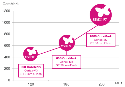
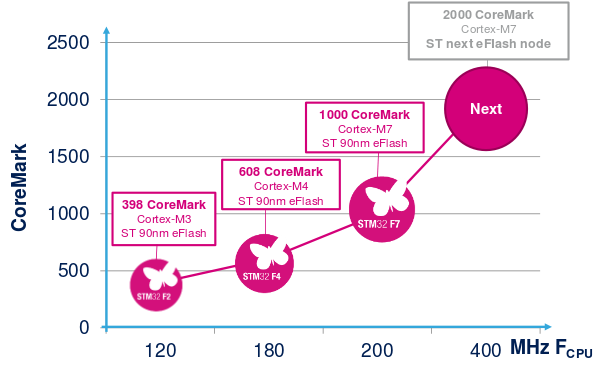
Taking advantage of ST’s ART Accelerator™ as well as an L1 cache, the STM32 F7 devices deliver the maximum theoretical performance of the Cortex-M7 no matter whether code is executed from embedded Flash or external Memory: 1000 CoreMark 428 DMIPS at 200 MHz fCPU.
The future performances
The M7 also provides the same C-friendly programmer's model and is binary compatible with existing Cortex-M processors.
Ecosystem and software compatibility enables simple migration from any existing Cortex-M core to the new Cortex-M7. System designers can therefore take advantage of extensive code reuse which in turn offers lower development and maintenance costs.
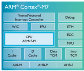
Cortex-M7 features:
Smart architecture with new peripheral set:
The STM32 F7 series unleashes the new Cortex M7 core:
-
Eva-Boards
STM32 Page
INDEX
STM32F7xx official page is here
- Introduction
- ARM Cortex-M7 official doc
- STM32F7 video presentation

- Cortex-M7 features
- Best performances
- Power efficiency
- Compatibility
- The future performances
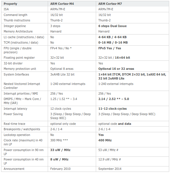
- Comparison: F4 vs F7
- Comparing Cortex-M Processors
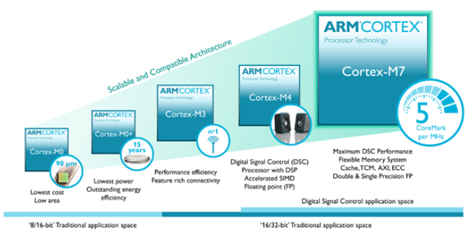
- What is Cortex M7
- Portfolio
- STM32F7xxx MKT presentation
- Da Cortex-M4 a Cortex-M7, migrare il codice è semplice con i consigli di Keil (in Italian language)
- Migrating Application Code from ARM Cortex M4 to Cortex M7 Processors
- Eva-Boards
- Tutorial
- LINK
INTRODUCTION
-
STM32F7xxx is ARM® Cortex®-M7 processor brings high performance and efficient digital signal processing to enable devices featuring superior embedded intelligence across the industrial, infrastructure and domestic sectors.
-
STM32F7 video presentation is here.
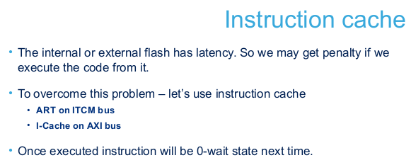
Thanks to their smart architecture with ST’s ART Accelerator™ and an L1 cache,
STM32F7 MCUs deliver the full performance of the ARM® Cortex®-M7 core
with code executed from either embedded Flash memory or an external
memory, reaching 1082 CoreMark at 216 MHz.
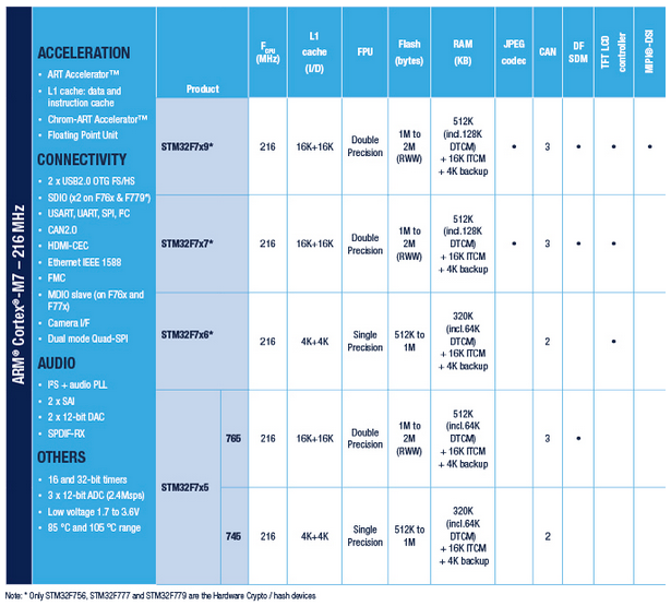
Two product lines with up to 1 Mbyte of Flash memory are available; the STM32F745 line and the STM32F746/756 line with TFT controller and hardware cryptography acceleration.
Packages range from 100 to 216 pins with sizes as small as 4.5 x 5.5 mm.
Learn about the STM32F7 series’ benefits in this e-presentation.
Key characteristics of the Cortex M7 processor include:
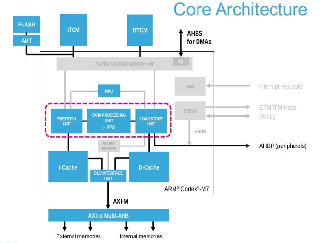
- High performance 6 stage pipeline with dual-issue (it executes up to two instructions per clock cycle)
- A 64bit AXI bus interface as the system bus
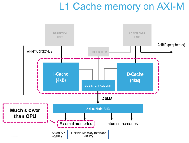
- Optional instruction cache (4 to 64KB) and data cache (4 to 64KB), with optional ECC (Error Correction Code) support for each of the cache memories.
- Optional 64bit Instruction Tightly Coupled Memory (I -TCM), and optional dual 32bit Data TCM (D-TCM), with support for a custom ECC implementation for each of the TCM interfaces
- Optional low - latency AHB peripheral bus interface (referred as AHBP in ARM documents)
- Integrated Nested Vectored Interrupt Controller (NVIC) with 1 to 240 interrupts with 3 to 8bit programmable priority level registers
- Optional Memory Protection Unit (MPU) with 8 or 16 regions
- Optional Floating Point Unit (FPU) with support for single - and double - precision floating point instructions
- Support for sleep modes and various low power mplementation technologies
- Powerful debug features, with optional full instruction and data trace
Taking advantage of ST’s ART Accelerator™ as well as an L1 cache, the STM32 F7 devices deliver the maximum theoretical performance of the Cortex-M7 no matter whether code is executed from embedded Flash or external Memory: 1000 CoreMark 428 DMIPS at 200 MHz fCPU.
The future performances
The M7 also provides the same C-friendly programmer's model and is binary compatible with existing Cortex-M processors.
Ecosystem and software compatibility enables simple migration from any existing Cortex-M core to the new Cortex-M7. System designers can therefore take advantage of extensive code reuse which in turn offers lower development and maintenance costs.
Cortex-M7 features:
- Six stage, superscalar pipeline delivering 2000 Coremarks at 400MHz in a 40LP process
- AXI interconnect (supports 64-bit transfer) and fully integrated optional caches for instruction and data allowing efficient access to large external memories and powerful peripherals
- Tightly coupled memory interfaces for rapid, real-time response
- Extensive implementation configurability to enable a wide range of cost and performance points to be targeted
- Optional full instruction and data trace via the Embedded Trace Macrocell enabling greater system visibility
- An optional safety package and built-in fault detection features contribute toward ASIL D and SIL 3 compliance, meaning Cortex-M7 is the perfect choice for companies targeting safety-related markets including automotive, industrial, transport and medical applications
- Widest third-party tools, RTOS, middleware support of any architecture, provided by the ARM Connected Community of complementary partner companies.
- 64-bit AMBA4 AXI, AHB peripheral port (64MB to 512MB)
- FPU - Floating Point Unit
Single and double precision floating point unit IEEE 754 compliant. Up to now the STM32F7 support Single FPU
- DSP
Single cycle 16/32-bit MAC
Single cycle dual 16-bit MAC
8/16-bit SIMD arithmetic
Hardware Divide (2-12 Cycles)
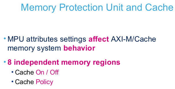
- MPU - 8 or 16 region MPU with sub regions and background region
- Bit Manipulation - Integrated Instructions & Bit Banding
- Pipeline 6-stage superscalar + branch prediction
Smart architecture with new peripheral set:
The STM32 F7 series unleashes the new Cortex M7 core:
- AXI and multi-AHB bus matrix for interconnecting Core, peripherals and memories
- Two general purpose DMA controllers and dedicated DMAs for Ethernet, high-speed USB On-The-Go and the Chrom-ART graphic accelerator.
- Peripheral speed independent from CPU speed (dual clock support) allowing system clock changes without impacting the function of the peripherals
- Even more peripherals, such as two serial audio interfaces (SAI) with SPDIF output support, three I2S half-duplex with SPDIF input support, two USB OTG with dedicated power supply and Dual Quad SPI interface
- LCD parallel interface, 8080/6800 modes
- LCD-TFT controller up to XGA resolution with dedicated Chrom-ART Accelerator™ for enhanced graphic content creation (DMA2D)
- Up to 25 communication interfaces
Up to 4× I2C interfaces (SMBus/PMBus)
Up to 4 USARTs 4 UARTs (12.5 Mbit/s, ISO7816 interface, LIN, IrDA, modem control)
Up to 6 SPIs (up to 50 Mbits/s), 3 with muxed simplex I2S for audio class accuracy via internal audio PLL or external clock
2 x SAI (serial audio interface)
2 × CAN (2.0B Active) and SDMMC interface
SPDIF-IN interface
HDMI-CEC
- Advanced connectivity
USB 2.0 full-speed device/host/OTG controller with on-chip PHY
USB 2.0 high-speed/full-speed device/host/OTG controller with dedicated DMA, on-chip full-speed PHY and ULPI
10/100 Ethernet MAC with dedicated DMA: supports IEEE 1588v2 hardware, MII/RMII
- 8- to 14-bit parallel camera interface up to 54 Mbytes/s
- Cryptographic acceleration: hardware acceleration for:
AES 128, 192, 256, Triple DES, HASH (MD5, SHA-1, SHA-2), and HMAC - True random number generator
- CRC calculation unit
- RTC: subsecond accuracy, hardware calendar
- 96-bit unique ID
- 3×12-bit, 2.4 MSPS ADC: up to 24 channels and 7.2 MSPS in triple interleaved mode
- 2×12-bit D/A converters
- Up to 18 timers: up to thirteen 16-bit (1x low power 16-bit timer available in stop mode) and two 32-bit timers, each with up to 4 IC/OC/PWM or pulse counter and quadrature (incremental) encoder input.
All 15 timers running up to 200 MHz. 2x watchdogs, SysTick timer
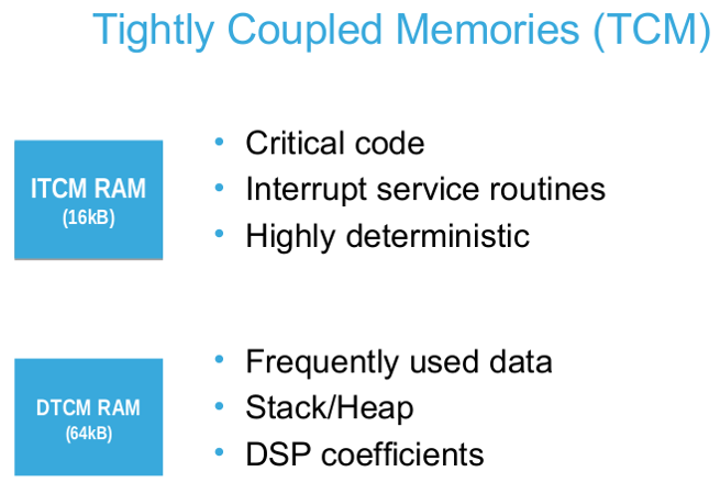
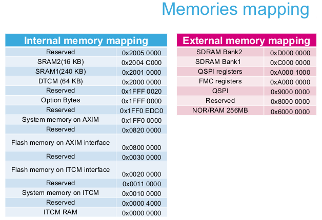
- 320KBytes of SRAM with scattered architecture:
- 240 Kbytes of universal data memory
- a 16 Kbytes partition for sharing data over the bus matrix
- 64 Kbytes of Tightly-Coupled Data Memory (DTCM) for time critical data handling (stack, heap...)
- 16 Kbytes of Tightly-Coupled Instruction Memory (ITCM) for time critical routines
- 4 Kbytes of backup SRAM to keep data in the lowest power modes.
- etc....
-
Power efficiency
-
Compatibility:
Power efficiency
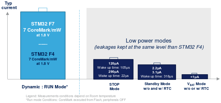
- 7 CoreMark/mW at 1.8V and 180 MHz
- 120µA typical current consumption in Stop mode with all context and SRAM saved
-
Compatibility:
- Cortex M7 is backward compatible with Cortex M4 instruction set
- STM32 F7 series is pin-to-pin compatible to the STM32 F4 series
-
Eva-Boards
- s
STM32F746G-DISCO
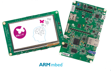
Key Features
STM32F746NGH6 microcontroller featuring 1 Mbytes of Flash memory and 340 Kbytes of RAM, in
BGA216 package
On-board ST-LINK/V2-1 supporting USB re-enumeration capability
USB functions: virtual COM port, mass storage, debug port
4.3-inch 480x272 color LCD-TFT with capacitive touch screen
Camera connector
SAI audio codec
Audio line in and line out jack
Stereo speaker outputs
Two ST MEMS microphones
SPDIF RCA input connector
Two pushbuttons (user and reset)
128-Mbit Quad-SPI Flash memory
128-Mbit SDRAM (64 Mbits accessible)
Connector for microSD card
RF-EEPROM daughterboard connector
USB OTG HS with Micro-AB connectors
USB OTG FS with Micro-AB connectors
Ethernet connector compliant with IEEE-802.3-2002
Five power supply options:
ST LINK/V2-1
USB FS connector
USB HS connector
VIN from Arduino connector
External 5 V from connector
Power supply output for external applications: 3.3 V or 5 V
Arduino Uno V3 connectors
Comprehensive free software including a variety of examples, part of STM32Cube package
- a
STM32756G-EVAL
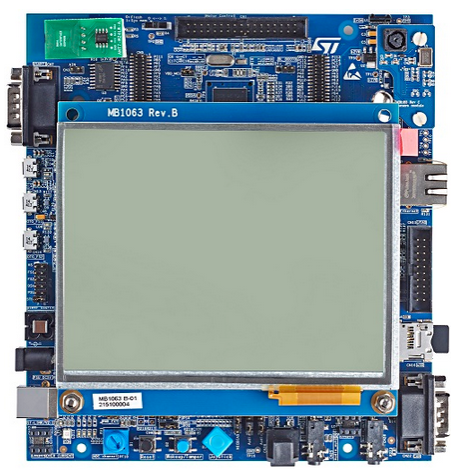
Key Features
STM32F756NGH6 microcontroller with 1 Mbyte Flash and 320+4 Kbytes RAM
Six 5 V power supply options:
Power jack
ST-LINK/V2-1 USB connector
User USB HS connector
User USB FS1 connector
User USB FS2 connector
Daughterboard
SAI Audio DAC, stereo audio jack which supports headset with microphone
Stereo digital microphone, audio jack connector used to connect external speakers
2 Gbytes (or more) SDMMC interface microSD card
RF-EEPROM on I2C compatible serial interface
RS-232 communication
IrDA transceiver
JTAG/SWD and ETM trace debug support, ST-LINK/V2-1 embedded
IEEE-802.3-2002 compliant Ethernet connector
Camera module
8Mx32bit SDRAM, 1Mx16bit SRAM & 8Mx16bit Nor Flash
512 Mbits QuadSPI Nor Flash
5.7 inch 640x480 pixel TFT color LCD with capacitive touch panel
Joystick with 4-direction control and selector.
Reset, WakeUp/Tamper or key button
4 color user LEDs
Extension connectors and memory connectors for daughterboard or wrapping board
USB OTG HS and FS with Micro-AB connectors
RTC with backup battery
CAN 2.0A/B compliant connection
Potentiometer
Motor control connector
L
Tutorial
Tutorial
- Some important AN:
- STM32F7 Series system architecture and performance (AN4667)
- Floating point unit demonstration on STM32 microcontrollers (AN4044)
- Digital signal processing for STM32 microcontrollers using CMSIS (AN4841)
- Some important tips concerning the STM32F7 (Cortex M7).
- STM32F7-Training 09/2015 - PoliTO (all documentations and Hands-On are free - we used the KEIL IDE)
- STM32F7-Training 06/2015 (we used the IAR IDE)
This training cover this topics:
It also contain this examples (for IAR 30 days full version):
IMPORTANT NOTE
- At the moment, the STM32F7-Training 06/2015, is only for SILICA/STM customers.
- If you are SILICA customer send me an email and ask me:
STM32F7-Training 06/2015
please specify also your City, Country and your contact in SILICA. - If you are STM customer please contact directly your local office of STM.
-
Some important tips concerning the STM32F7
Some important tips concerning the STM32F7
M7 Core
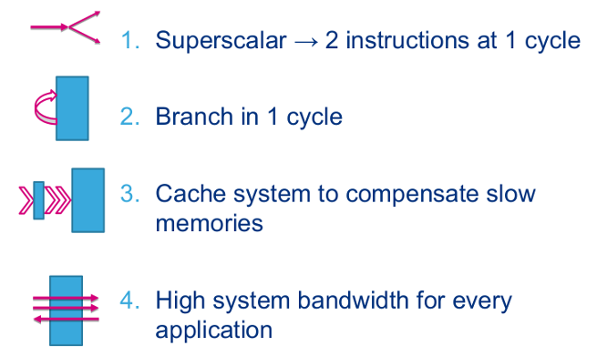
The instruction set of M7 are the same of M4 (see below), but a big difference is a High performance 6 stage pipeline with dual-issue (it executes up to two instructions per clock cycle).
M7 is a superscalar MCU, this means that it has the possibility to execute two instruction every clock cycle.
In other word means that Cortex M7 fetch from flash at 64bit.
But for reach this performance is very important that the compiler is a clever compiler, this because M7 has the possibility to execute (in the same time) one of this instructions; see the red box below.
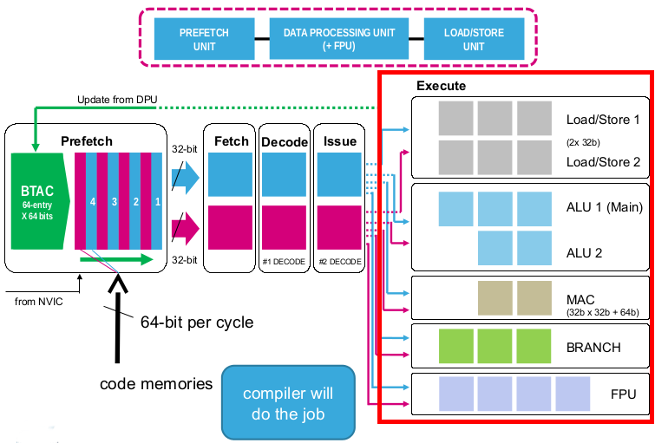
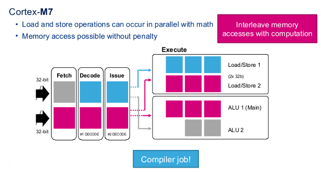
If the compiler write on two sequentially 32bit of flash, two load instructions, the M7 execute the first load and at the next clock cycle the second load... you have lost the possibility to execute two instruction every machine cycle.
At the moment (October 2015), for reach the performance from L1 or TCM memory, you must manually write the necessary instructions.
See the MPU instructions, in the Hands-On sections.
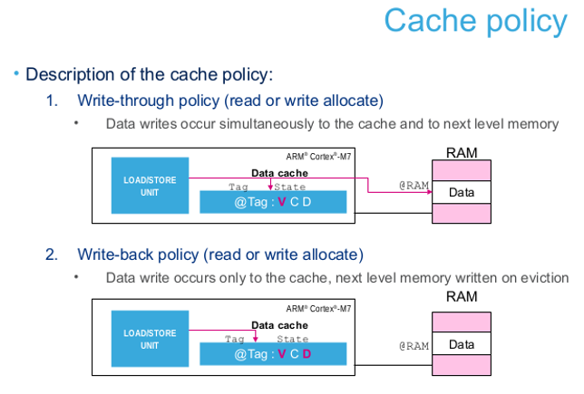
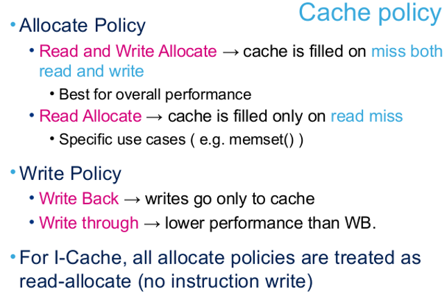
There are some examples concerning Cache, ITCM, DTCM, etc, in the Hands-On of this training.
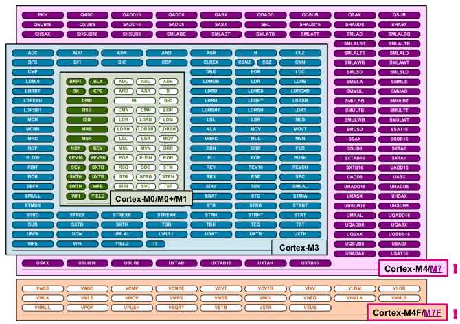
ARM Cortex-Mx acronyms
The instruction set of M7 are the same of M4 (see below), but a big difference is a High performance 6 stage pipeline with dual-issue (it executes up to two instructions per clock cycle).
M7 is a superscalar MCU, this means that it has the possibility to execute two instruction every clock cycle.
In other word means that Cortex M7 fetch from flash at 64bit.
But for reach this performance is very important that the compiler is a clever compiler, this because M7 has the possibility to execute (in the same time) one of this instructions; see the red box below.
If the compiler write on two sequentially 32bit of flash, two load instructions, the M7 execute the first load and at the next clock cycle the second load... you have lost the possibility to execute two instruction every machine cycle.
At the moment (October 2015), for reach the performance from L1 or TCM memory, you must manually write the necessary instructions.
See the MPU instructions, in the Hands-On sections.
There are some examples concerning Cache, ITCM, DTCM, etc, in the Hands-On of this training.
ARM Cortex-Mx acronyms
ALU = Arithmetic Logic Unit
SIMD = Single instruction, multiple data
MPU = Memory Protection Unit
MAC = multiply–accumulate operation
LSU = load store unit
DPU = data processing unit
DTCM & ITCM = The memory system includes support for the connection of local Tightly Coupled Memory called ITCM (16K) and DTCM (64K)
STB = store buffer
BUI = Bus Interface Unit
TCU = Tightly-Coupled interface Unit
EPPB = External Private Peripheral Bus-The APB External PPB
Superscalar architecture first appeared on Intel Pentium 5 in 1993 => it means it is able to process multiple instructions in parallel (in our case, Cortex M7, up to 2, that’s why dual-issue)
-
LINK
LINK
- STM32 F7 Series - The smartest STM32 ever: World’s 1st ARM® Cortex® -M7 based 32-bit MCU (on YouTube)
- ARM Cortex-M7: Digital Signal Processing Drives Family Evolution
- ARM gives Internet of Things a piece of its mind – the Cortex-M7
- STMicro, ARM do a double whammy with new Cortex-M7 core
- Cortex-M7 Launches: Embedded, IoT and Wearables